30+ asic design flow block diagram
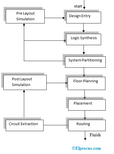
This order of steps is known as ASIC Design Flow. An FPGA Field Programmable Gate Arrays is a programmable chip used in various industry applications such as 4G5G Wireless systems Signal Processing Systems and.
Ai Edge Chips Nvidia Jetson Xavier Nx Agx Xavier Google Coral Edge Tpu Startups By Jonathan Hui Aug 2020 Medium Medium
FPGA designs often start with what are called reference designs which represent a technical blueprint of a system that is intended for others.
. Or b explain the asic design flow with a neat diagram. Ad Templates Tools To Make Block Diagrams. EnSilica offers full-flow design services focused on supporting companies with their own IC design teams to develop ASIC and FPGA based products.
School Dayananda Sagar College Of Education. OR b Explain the ASIC design flow with a neat diagram Enumerate clearly the. Sum A B.
A time interval is characterized by two events the start and stop events corresponding to the. Asic design flow mentor graphics cad tools select from eda list in user-setup on the sun network icflow20072 for custom standard cell ic designs ic flow tools design architect-ic. Steps of design flow are given in below flow chart.
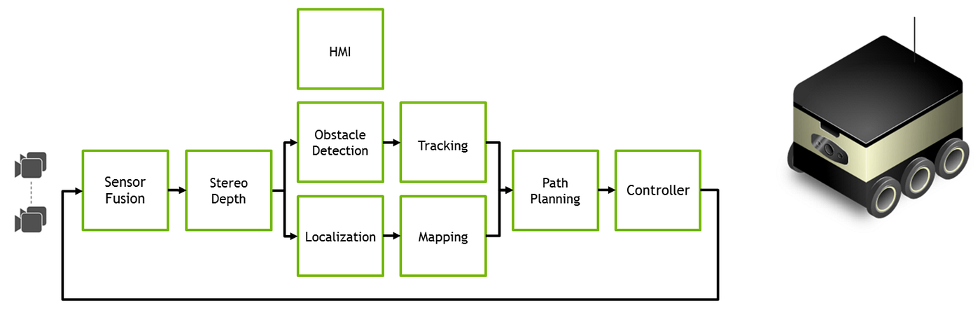
Designing an ASIC is carried out in step by step manner. Modern Design Flow of FPGAs. A block diagram depicting the overview of the implemented TDC architecture is presented in Fig.
ASIC Design Flow Design. In the half adder circuit the sum and carry bits are defined as. The design flow described in this document consists of five major procedures as shown in Figure 1 Functional Design Synthesis Place Route System.
The corresponding boolean expressions are given here to construct a ripple carry adder. Clock tree synthesis and reset is routed. Camo Library Development integration with a typical ASIC design flow.
ASIC IC Design Services. Functional Software Electrical etc. After this each block is routed.
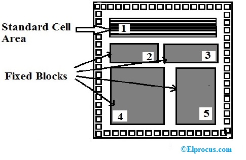
Blocks include IP and user -created modules Create a chip floor plan from the schematic Place functional blocks and IO pads Connections shown as overflows Route top-level connections. Timeless developed a complete asic flow.

A Signal Diagram Of A Multiplier Block For R G B Color Channels B Download Scientific Diagram
Application Specific Integrated Circuit Types And Applications

Trending Ic Design Directions In 2022
2
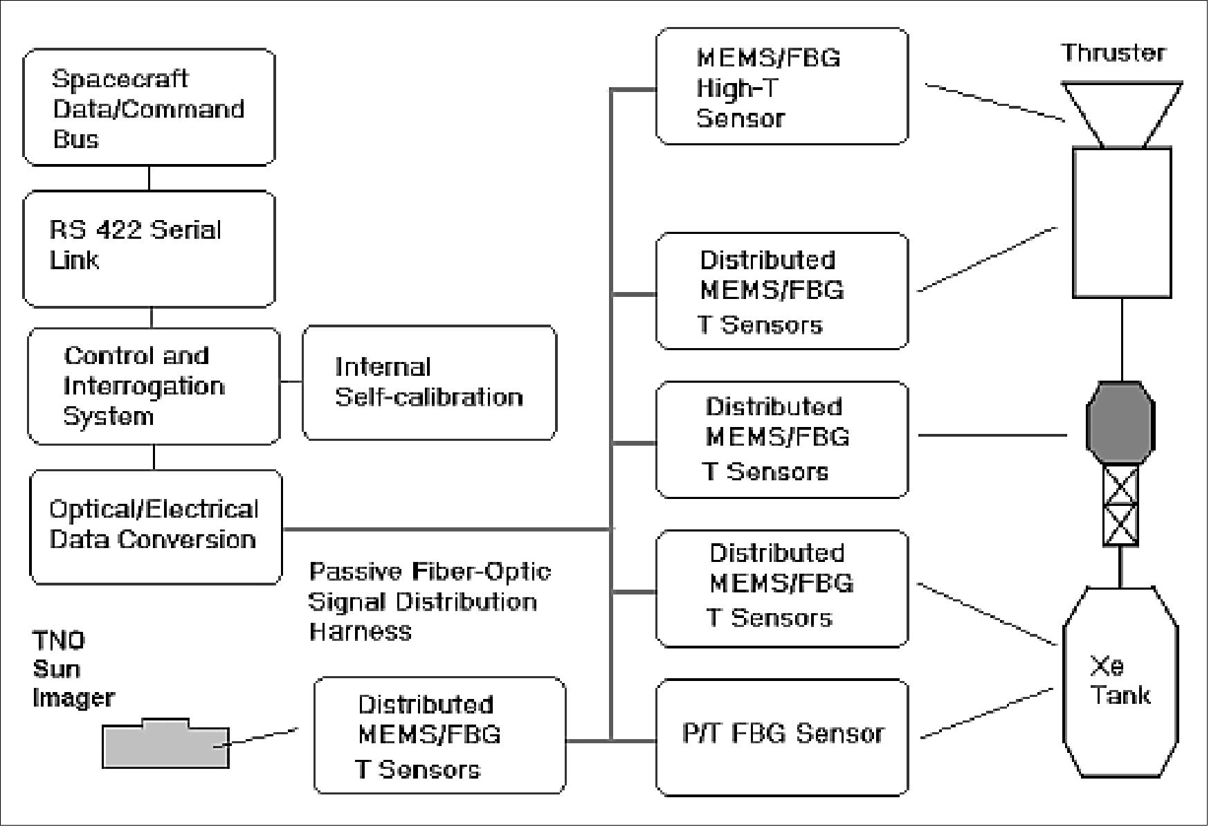
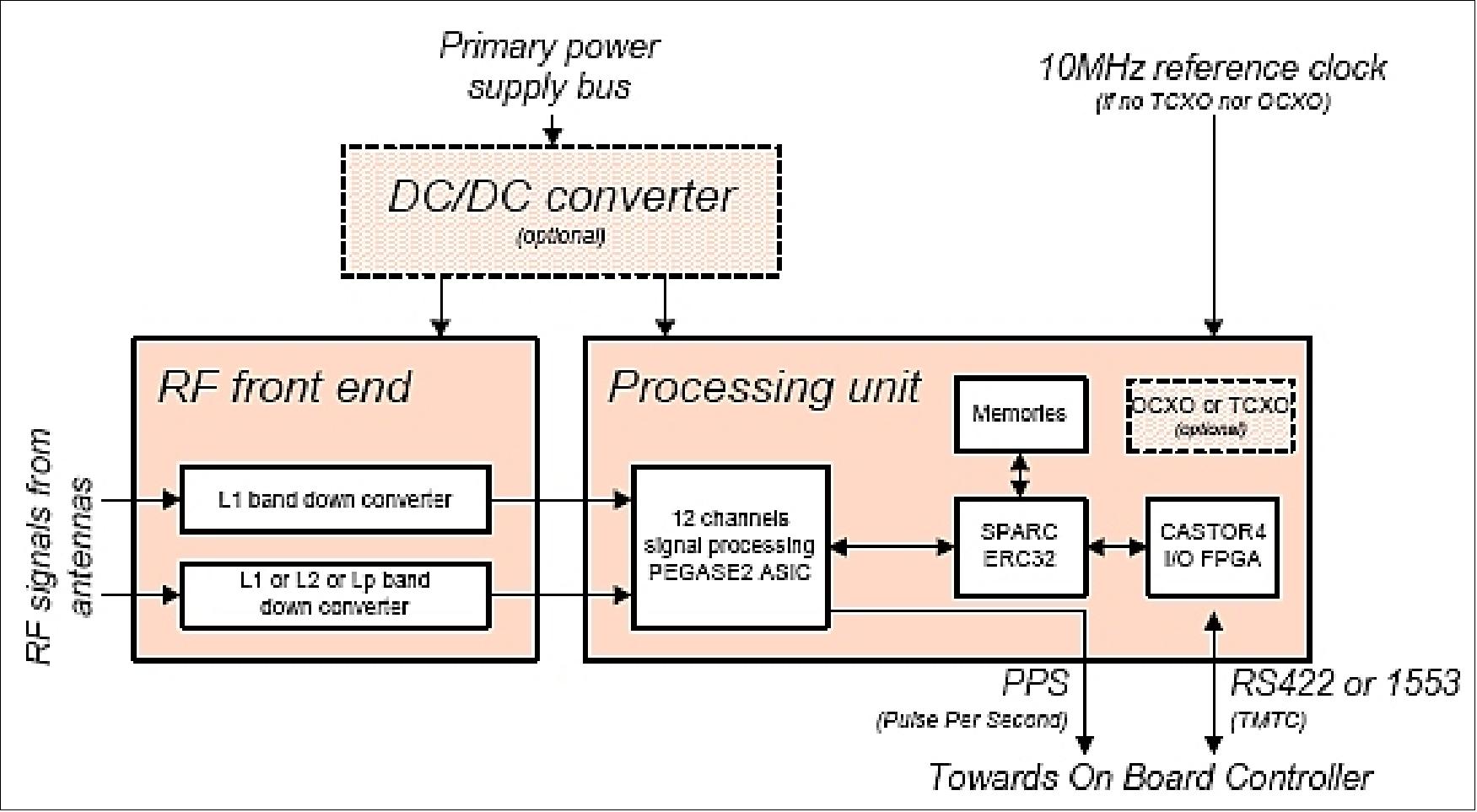
Proba 2
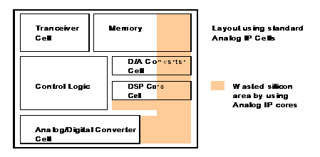
Demystifying Analog Mixed Signal Asics Anysilicon
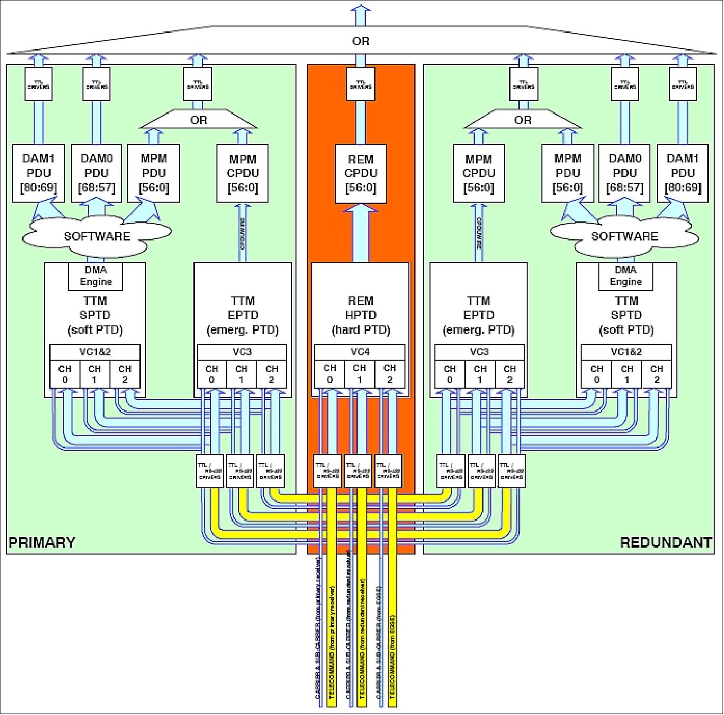
Proba 2

Trending Ic Design Directions In 2022
Proba 2
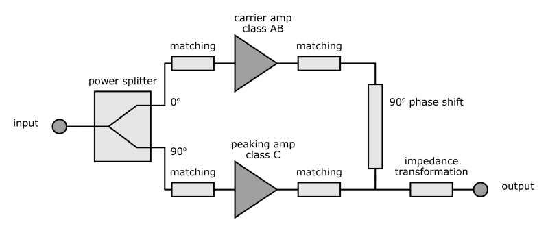
The Art Of Designing And Building Rf Power Amplifier Applications Bits Chips

Trending Ic Design Directions In 2022

What Challenging Projects Are Given To Vlsi Design Engineers In Companies Like Xilinx And Qualcomm Quora
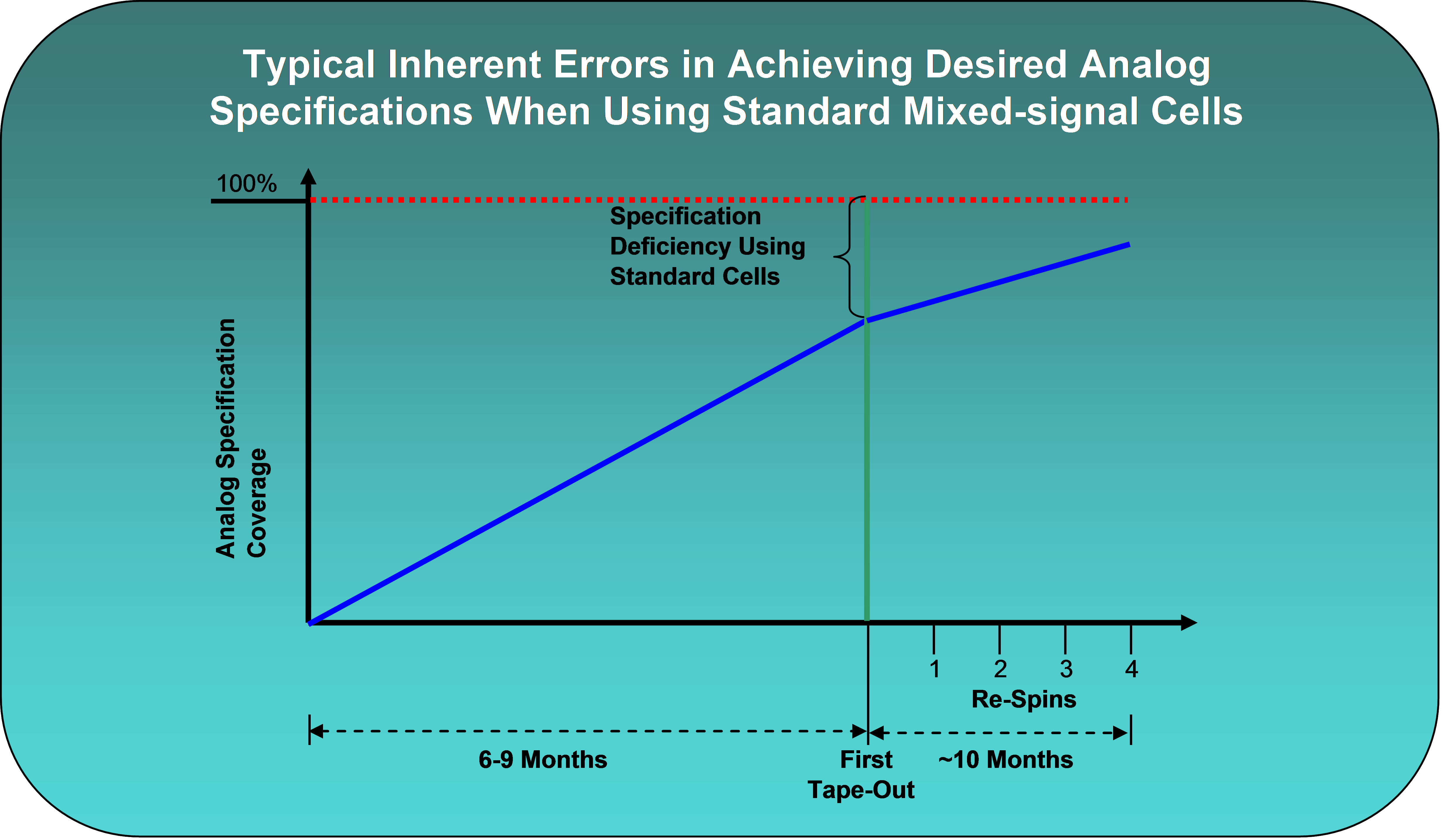
Demystifying Analog Mixed Signal Asics Anysilicon

Thermo Fisher Scientific Develops An Appetite For Modeling Bits Chips
Application Specific Integrated Circuit Types And Applications
Application Specific Integrated Circuit Types And Applications
Javascript Block Diagrams For Simple Visualization Dhtmlx